What Should Engineers Look for in a High-Performance Wafer Handling Solution?
Posted by Kensington Laboratories
Filed in Business 247 views
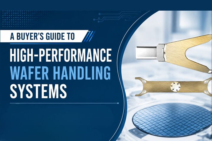
With the transition to smaller process nodes, advanced packaging and AI-based chip manufacturing the demands on wafer handling solutions have never been greater. Precision, repeatability and control of contamination are no longer desirable features but imperatives. The first step to choose the right system is to evaluate each component involved in the wafer moving, especially the component that directly contacts and transfers sensitive wafers throughout the manufacturing process.
A high-performance handling system affects more than handling accuracy. It influences particle generation, wafer stability, cycle time and overall equipment reliability. Fabs run 24/7 today and engineers need solutions that can deliver consistent performance and flex to meet shifting production demands.
Key Features Engineers Should Evaluate
Before selecting a wafer handling system, engineers should carefully evaluate the wafer end effector along with other critical technical factors.
High positioning accuracy: The system is expected to align wafers with micron level precision to minimize the alignment errors.
Low particle generation: Materials and surface finishes shall be cleanroom compatible and minimize contamination.
Safe Handling: Firm wafer grip to minimize risk of slippage, edge chipping or wafer breakage.
Multiple-wafer-size compatibility: Flexible designs simplify future equipment upgrades.
Continuous operation: Components must withstand high-cycle production with minimum maintenance.
These characteristics are important to keep an efficient semiconductor wafer handling and to protect valuable wafers in the production process.
Why Integration Is Important
Robotic wafer handling systems are being used more and more in modern fabs to communicate with automated manufacturing equipment. The handling solution has to be integrated with robotic arms, inspection tools and process equipment, without creating bottlenecks in production.
Equally important is the selection of the right End-of-arm tooling. The lightweight design, balanced construction and application-specific geometry all contribute to increased robot performance and minimum vibration and handling errors.
Industry Trends Shaping Wafer Handling
Recent investments in AI chip manufacturing, advanced packaging and smart semiconductor factories are generating demand for faster, cleaner and more intelligent automation. Manufacturers are focusing more on predictive maintenance, digital monitoring and precision robotics to increase yield and reduce equipment downtime. As the wafer geometries become more complex, the handling systems need to deliver greater accuracy without sacrificing the throughput.
Final Thoughts
A wafer handling solution is not just about speed. Precision, cleanliness, integration capability and long-term reliability provide consistent manufacturing performance. By carefully evaluating system design and selecting the proper wafer end effector, engineers can improve wafer protection, increase production efficiency and set up their facilities for the next generation of semiconductor manufacturing.