How Robotic Automation Increases Productivity in Cleanroom Manufacturing
Posted by Kensington Laboratories
Filed in Business 23 views
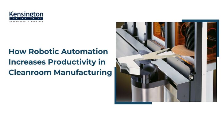
Human operators remain the single largest source of particulate contamination in controlled environments. With microchip fabrication technology scaling down to less than 3nm, even the smallest skin cell or textile fiber can jeopardize an entire batch of wafers. Using semiconductor automation solutions will reduce the human error factor while guaranteeing consistent yield output around the clock.
Eliminating Contamination and Yield Loss
Deploying specialized cleanroom automation shifts human operators out of active processing zones and into supervisory roles. Modern robotic handling systems operate continuously inside ISO Class 1 enclosures without generating particulate shedding or outgassing. This maintains the strict environmental purity that advanced lithography and etch nodes demand, protecting wafer integrity at every stage.
Key operational advantages of automated material transfer include-
-
Particle Isolation- Human personnel generate up to 70% of all cleanrooms particulate contamination through shedding and physical movement. Automated robotics isolate delicate substrates from direct human exposure entirely.
-
Complex Spatial Reach- Utilizing multi-link robots allows wafer transfer arms to navigate tight tool-to-tool footprints, optimizing internal fab space without disrupting critical laminar airflow patterns.
-
Process Repeatability- Standardized robotic trajectories prevent micro-vibrations, thermal fluctuations, and physical misalignments that frequently cause wafer edge damage or Cassette-to-Cassette handling errors.
Maximizing Throughput and Line Utilization
Implementing industrial robotics in high-volume semiconductor fab lines ensures continuity of operation across all shifts. Manual lot handling often leads to uneven tool queues, uncoordinated batch transfers, and long idle times between critical process steps. Automated overhead hoist transport routes, automated guided vehicles, and tool-mounted manipulators guarantee a smooth, real-time material flow throughout the entire facility without human intervention.
Facilities are systematically eliminating expensive production bottlenecks with advanced semiconductor automation solutions. Automated systems perform wafer transfer, carrier loading, and reticle positioning with sub-millimeter accuracy, directly increasing overall manufacturing efficiency. Cleanroom robotics in fabs enables tool utilization rates up to 20% higher and reduces material transport delays by more than 50% compared to traditional manual transfer models.
To Sum It Up
There is no tolerance for particle-induced defects or unscheduled tool downtime in today’s chip manufacturing economy. Moving from manual handling to scalable semiconductor automation solutions ensures that the valuable substrates are not contaminated and allows the process to reach maximum wafer production each day. Integrating specialized robotics technology helps companies achieve better yields, improved consistency, and a scalable architecture for future semiconductor manufacturing.