Can the Package Substrates Market Reach USD 22.19 Billion by 2033 at 8.7% CAGR?
Posted by shraddha thakur
Filed in Technology 352 views
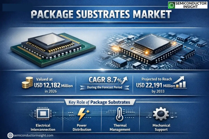
Global Package Substrates Market was valued at USD 12.18 billion in 2026 and is projected to reach USD 22.19 billion by 2033, registering a Compound Annual Growth Rate (CAGR) of 8.7% over the forecast period 2026–2034. This robust expansion trajectory is underpinned by accelerating investment in artificial intelligence infrastructure, next-generation data center architectures, and the proliferation of heterogeneous chip integration technologies that demand increasingly sophisticated substrate solutions.
Package substrates are precision-engineered multilayer interconnect structures that serve as the critical electrical and mechanical interface between semiconductor dies and printed circuit boards. Far more than passive carriers, modern package substrates perform four simultaneous engineering functions — electrical signal routing at fine line/space geometries, power distribution with minimal impedance, thermal dissipation away from the die junction, and mechanical support to protect fragile silicon from environmental and handling stress
👉 Access the complete industry analysis and demand forecasts here: https://semiconductorinsight.com/report/package-substrates-market/
Market Definition and Dynamics
The package substrate market sits at a structural inflection point driven by two converging forces: the physical limits of monolithic chip scaling and the exponential growth of compute-intensive AI workloads. As transistor density improvements under Moore's Law have slowed, the semiconductor industry has pivoted toward advanced packaging — chiplet disaggregation, 2.5D interposer-based integration, and 3D stacking .
Market Drivers
• AI Infrastructure Buildout and Hyperscale Data Center Expansion:
• 5G Network Densification and mmWave Infrastructure Deployment:
Market Restraints
• Prohibitive R&D and Capacity Investment Requirements
• Geographic Supply Concentration and Geopolitical Exposure
• Manufacturing Complexity and Yield Challenges at Advanced Geometries
Market Opportunities
• Fan-Out Panel-Level Packaging Technology Adoption: The commercialization of fan-out panel-level packaging presents a transformative cost reduction pathway
• Glass-Core Substrate Development for Next-Generation Performance: Glass-core substrates offer compelling advantages over organic counterparts for ultra-high-frequency and extreme-density applications
Competitive Landscape
List of Key Package Substrates Companies
• Unimicron
• Ibiden
• Nan Ya PCB
• Shinko Electric Industries
• Kinsus Interconnect Technology
• AT&S
• Samsung Electro-Mechanics
• Kyocera
• Toppan
• Zhen Ding Technology
• Daeduck Electronics
• LG InnoTek
• Shennan Circuit
• Simmtech
• ASE Material
Segment Analysis
By Type
• FCBGA Substrate
• FCCSP Substrate
• WB-CSP/BGA
By Application
• Server/Data Center
• AI/HPC Chips
• Smartphone
• Automotive Electronics
Regional Insights
Asia-Pacific holds an essentially uncontested dominant position in global package substrate production and consumption, with Taiwan, South Korea, Japan, and China collectively accounting for over 90% of manufacturing capacity and hosting the dense ecosystem of foundries, OSATs, substrate material suppliers, and end-product assemblers that makes the region a self-reinforcing production hub.
Your Competitive Edge Starts with Better Intelligence — Explore the Full Package Substrates Report
In a market this concentrated and technically complex, the difference between a strategic win and a missed opportunity is the quality of your market intelligence. Our comprehensive Package Substrates Market report delivers the segment-level forecasts, technology roadmap analysis, competitive benchmarking, and regional capacity data that procurement leaders, investors, and technology strategists need to act with precision.
👉 Unlock the complete market intelligence report — forecasts, competitive dynamics, and technology trends through 2034: https://semiconductorinsight.com/report/package-substrates-market/
📄 Download your no-cost sample report today — examine segment breakdowns and supplier positioning before committing to the full analysis: https://semiconductorinsight.com/download-sample-report/?product_id=133388
About Semiconductor Insight
Semiconductor Insight is a global intelligence platform delivering data-driven market insights, technology analysis, and competitive intelligence across the semiconductor and advanced electronics ecosystem. Our reports support OEMs, investors, policymakers, and industry leaders in identifying high-growth markets and strategic opportunities shaping the future of electronics.
🌐 https://semiconductorinsight.com/
🔗 LinkedIn: Follow Us
📞 International Support: +91 8087 99 2013