Understanding EFEM Design: Key Component Driving Wafer Automation
Posted by Kensington Laboratories
Filed in Technology 421 views
In semiconductor fabrication, accuracy and cleanliness cannot be overlooked. This is when the importance of EFEM wafer automation comes into play. With the use of efem wafer automation technology, wafers can be moved with precision and rapidity without compromising on cleanliness. The more advanced semiconductor manufacturing processes become, the greater becomes the significance of efem technology.
What Is an EFEM and Why It Matters
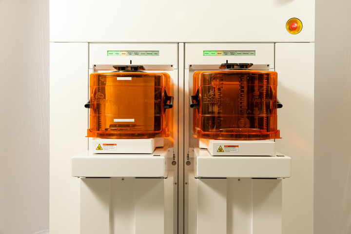
An Equipment Front End Module acts as the critical interface between fabrication equipment and automated material handling systems. It ensures wafers are loaded, aligned, and transferred in a controlled microenvironment before entering processing tools such as lithography or etching systems.
In modern EFEM wafer automation, these modules are not standalone, they are integrated into larger cleanroom automation systems. Their key responsibility is to ensure that wafers are ready for processing with less contamination and uniformity through different production lines.
How EFEM Supports Wafer Handling Automation
The importance of wafer handling automation lies in eliminating human contact and reducing variability. An efem system enables this by coordinating multiple components that work together to manage wafer flow efficiently.
Key benefits include:
-
Reduced contamination through controlled environments
-
Improved process consistency
-
Faster wafer transfer between tools
-
Enhanced production reliability
By integrating with semiconductor load port systems and robotics, EFEMs ensure smooth and uninterrupted operations.
Core Components of EFEM Systems
Although EFEMs include several elements, three components form the backbone of effective EFEM wafer automation:
1. Semiconductor Load Port Systems
Load ports serve as the entry point for wafer carriers such as FOUPs or cassettes. They:
-
Securely dock carriers
-
Identify wafer lots
-
Enable safe loading and unloading
These systems are vital for retaining contamination-free transfer.
2. Wafer Transfer Robotics
Wafer transfer robotics handle the precise movement of wafers within the EFEM. These robots are designed for:
-
High-speed, multi-axis motion
-
Gentle handling of fragile wafers
-
Accurate placement within microns
They play a central role in ensuring both speed and precision.
3. Wafer Aligners
Aligners ensure wafers are correctly oriented before entering process chambers. Their functions include:
-
Detecting wafer notch or flat orientation
-
Correcting misalignment
-
Preparing wafers for accurate processing
Together, these components produce a seamless and reliable wafer transfer process.
Internal Architecture of EFEM Systems
To support advanced cleanroom automation systems, EFEMs are structured into three functional modules:
1. Microenvironment Control Module
This module maintains ultra-clean conditions required for semiconductor processes. It includes:
-
HEPA/ULPA filters for particle control
-
Chemical filters to remove contaminants
-
Ionizers to manage static charge
-
Controlled airflow systems
2. Automation Module
This module focuses on movement and coordination:
-
Wafer transfer robotics for handling
-
Aligners for positioning
-
Carrier systems for storage and transport
-
Sensors and safety systems for reliable operation
3. Software Control Module
Software is the backbone of intelligent automation. It manages:
-
Robot motion and coordination
-
Alignment accuracy
-
System monitoring and diagnostics
-
Integration with factory systems
This integration is critical for achieving efficient automated material handling systems.
EFEM vs Traditional Handling Systems
|
Feature |
Traditional Handling |
EFEM Wafer Automation |
|
Human Involvement |
Moderate to High |
Minimal |
|
Contamination Risk |
Higher |
Extremely Low |
|
Speed |
Limited |
High-speed automation |
|
Precision |
Variable |
Highly accurate |
|
Integration |
Basic |
Fully integrated with automation systems |
This comparison highlights why EFEM-based systems are essential for modern semiconductor production.
Why EFEM Design Drives Better Performance
A well-designed EFEM wafer automation system delivers several advantages:
-
Higher Throughput: Faster wafer movement reduces production delays
-
Improved Yield: Controlled environments minimize defects
-
Operational Efficiency: Automation diminishes manual intervention
-
Scalability: Easily incorporates with innovative fabrication processes
These benefits make EFEM systems a key investment for high-volume manufacturing environments.
The Role of EFEM in Future Semiconductor Automation
With the continual advancements in semiconductor technology, the need for intelligent wafer handling automation will grow further. The EFEM system is getting better through innovations like:
-
Robotic handling for sensitive wafer movement
-
Better compatibility with AI systems
-
Coordinated operation between various systems
Such technological developments will play an important role in designing the automated systems for cleanrooms of the future.
Conclusion
It is clear that EFEM systems play a vital role in today's wafer handling due to the fact that they offer precision, cleanliness, and efficiency during the process. Through their combination of semiconductor load port systems, wafer transfer robotics, and sophisticated control systems, EFEM wafer automation ensures an effective and reliable manufacturing process.
The move towards more innovative automation in the semiconductor manufacturing industry requires that companies put money into properly designed EFEM systems to stay competitive. Such companies as Kensington Laboratories have been established as credible providers of robotics and automation in the industry.