Wafer Hybrid Bonding Machine Market Projected to Reach USD 850 Million by 2034 Amid 3D IC Surge
Posted by shraddha thakur
Filed in Music 392 views
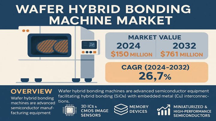
Global Wafer Hybrid Bonding Machine market was valued at USD 150 million in 2024 and is forecasted to attain USD 850 million by 2034, registering a CAGR of 26.7% during 2026-2034. This acceleration stems from escalating needs for high-density interconnects in AI accelerators and advanced memory stacks.
Wafer hybrid bonding machines execute dielectric-to-dielectric (SiO2) fusion with copper nano-pad compression at pitches under 1μm, achieving void-free bonds via plasma activation and annealing up to 300°C. These systems deliver alignment precisions below 100nm, enabling 10x higher I/O densities than TSVs while slashing resistance by 40% and power by 30%. Essential for stacking HBM dies with 100,000+ connections/mm², 3D logic-memory hybrids in HPC, CIS pixels at 0.7μm for automotive vision, and MEMS-photonics in LiDAR, they support 300mm wafers with throughputs over 50 pairs/hour.
👉 Access the complete industry analysis and demand forecasts here:
https://semiconductorinsight.com/report/wafer-hybrid-bonding-machine-market/
Market Definition and Dynamics
Heterogeneous integration mandates hybrid bonding as 2nm nodes demand sub-10μm pitches, with advanced packaging market eyeing USD 50 billion by 2025. Pivotal forces include AI chip complexity rising 35% CAGR and EV semiconductor uptake doubling to USD 80 billion.
Asia-Pacific fabs, 60% of capacity, leverage CHIPS-like subsidies while grappling with yield hurdles at 80-90%.
Market Drivers
- Advanced packaging shift enabling <10μm pitches for 3D ICs in HPC.
- AI/HBM stacks requiring 16+ layers with 30% power cuts.
- Automotive ADAS demanding reliable sensors under extremes.
Market Restraints
- USD 3-5 million unit costs plus cleanroom overheads.
- Yields at 80-90% versus 98% for legacy processes.
- Material CTE mismatches sparking 25% defects.
Market Opportunities
- Photonics for data center optics with <200nm alignment.
- Chiplet standards targeting <2μm interconnects.
- CXL/HBM4 memory exceeding 100k I/Os/mm².
Competitive Landscape
Consolidation intensifies with leaders at 60% share via AI-optimized tools cutting defects 20%. Innovations like EVG's GEMINI boost throughput 40% for HBM production.
List of Key Wafer Hybrid Bonding Machine Companies
- EV Group (EVG)
- SUSS MicroTec
- Genesem
- ASMPT
- C SUN
- Piotech
- Beijing U-Precision Tech
- Wisdom Semiconductor Technology
Segment Analysis
By Type
- Wafer-to-Wafer Hybrid Bonding
- Die-to-Wafer Hybrid Bonding
By Application
- CMOS Image Sensor (CIS)
- NAND Flash Memory
- DRAM
- High Bandwidth Memory (HBM)
- Others
Regional Insights
Asia-Pacific dominates at 60% share through China's USD 150 billion self-sufficiency drive and Taiwan/South Korea foundries scaling HBM, North America surges via USD 52 billion CHIPS for Intel/Micron, Europe excels in ADAS photonics led by Austria/Germany, with Middle East & Africa/South America nascent via defense and assembly hubs.
👉 Explore comprehensive forecasts, tech breakdowns, and rival intel:
https://semiconductorinsight.com/report/wafer-hybrid-bonding-machine-market/
📄 Claim your no-cost sample unpacking segments and geo-strategies:
https://semiconductorinsight.com/download-sample-report/?product_id=107195
About Semiconductor Insight
Semiconductor Insight is a global intelligence platform delivering data-driven market insights, technology analysis, and competitive intelligence across the semiconductor and advanced electronics ecosystem. Our reports support OEMs, investors, policymakers, and industry leaders in identifying high-growth markets and strategic opportunities shaping the future of electronics.
🌐 https://semiconductorinsight.com/
🔗 LinkedIn: Follow Us
📞 International Support: +91 8087 99 2013